In Semiconductor Industry, Packaging Failure Is Not Acceptable
Semiconductor equipment is not just expensive.
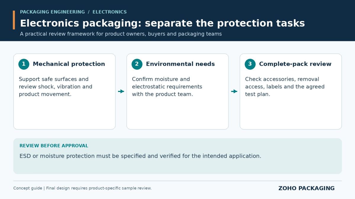 ESD or moisture protection must be specified and verified for the intended application.
It is:
- Precision-critical
- Calibration-sensitive
- High replacement cost
- Long lead-time equipment
👉 A single packaging failure can lead to:
- Equipment misalignment
- Recalibration cost
- Production delay
- Contract penalties
This is not packaging. This is risk management.
Typical Risks in Semiconductor Equipment Shipping
During export (especially sea freight), risks include:
- Micro-vibration affecting internal alignment
- Shock impact during handling
- Compression damage from stacking
- Moisture affecting sensitive components
- Static electricity damage (ESD)
👉 Most suppliers underestimate one thing:
Damage doesn’t always show outside.
It shows after installation.
Our Semiconductor Packaging Engineering System
We design packaging as a complete protection system, not just materials.
1. Vibration Isolation Design (核心)
Semiconductor equipment is highly sensitive to:
- Continuous low-frequency vibration
- Resonance amplification
We design:
- Floating cushioning systems
- Multi-layer damping structures
- Isolation-based support
👉 Goal:
Reduce vibration transmission, not just absorb shock.
2. Shockproof Protection (Impact Control)
- Drop impact simulation
- Corner & edge reinforcement
- Controlled deformation cushioning
👉 Designed to survive real handling conditions, not ideal ones.
3. Structural Load Design (Heavy Equipment Ready)
- High-strength corrugated + reinforcement
- Wooden crate / hybrid packaging options
- Load path engineering
👉 Key concept:
Load must travel through structure, not product.
4. ESD & Clean Protection
- Anti-static materials
- Clean packaging options
- Dust & contamination control
For:
- Wafer equipment
- PCB-related systems
- Cleanroom-sensitive components
5. Moisture & Export Protection
- Desiccant system integration
- Barrier packaging
- Sea freight environment design
👉 Especially critical for long-distance shipping.
Before vs After: Semiconductor Packaging Upgrade
Before (Standard Industrial Packaging):
- Basic carton / wooden box
- No vibration isolation
- No load calculation
👉 Result:
- Internal misalignment
- Calibration issues
- Hidden damage
After (Engineered Semiconductor Packaging):
- Isolation-based cushioning
- Load path design
- Full export condition simulation
👉 Result:
- Stable delivery
- No recalibration issue
- Reduced risk
Types of Equipment We Handle
- Semiconductor manufacturing equipment
- Wafer handling systems
- Precision optical equipment
- Cleanroom machinery
- High-value automation systems
Why High-End Clients Choose Zoho Packaging
✔ Engineering-based design (not material-based)
✔ Export-focused (sea + air)
✔ Experience with high-value equipment
✔ Fast prototyping & testing
✔ Flexible production (Taiwan-based factory)
👉 We don’t compete on price.
👉 We compete on risk reduction.
The Real Cost of Packaging Failure
For semiconductor equipment:
- Recalibration cost
- Downtime loss
- Contract penalty
- Reputation damage
👉 One failure can cost more than
an entire year of packaging budget.
Work With Us
If your equipment is:
- High value
- Precision sensitive
- Exported globally
You need packaging that is:
✔ Engineered
✔ Tested
✔ Reliable
👉 Contact us for semiconductor packaging consultation.
FAQ
1. Why is semiconductor packaging different from normal packaging?
Because semiconductor equipment is highly sensitive to vibration, shock, and environmental conditions. Standard packaging cannot provide sufficient protection.
2. What is vibration isolation in packaging?
It is a design method that reduces vibration transfer from external forces to the product using damping structures.
3. Do semiconductor products need anti-static packaging?
Yes. Many components are sensitive to electrostatic discharge (ESD), which can cause hidden damage.
4. Is wooden crate packaging necessary?
For heavy or high-value equipment, wooden or hybrid packaging is often required for structural strength.
5. What is the biggest risk during shipping?
Micro-vibration over long periods, which can cause internal misalignment.
6. Can packaging prevent calibration issues?
Yes. Proper vibration isolation design significantly reduces the risk of misalignment.
7. Do you provide custom solutions?
Yes. All packaging is designed based on product specs and shipping conditions.
8. How do you test packaging performance?
We use drop tests, load simulations, and vibration considerations based on real shipping conditions.
9. Can this be used for air freight?
Yes. We design packaging for both air and sea shipping conditions.
10. How do I start a project?
Provide product size, weight, and shipping method. We will propose a solution.
In semiconductor shipping,
damage is not visible — until it’s too late.